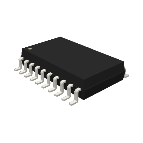
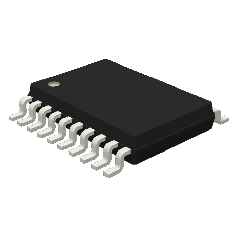
30V Quad-Channel Differential Line Driver(16 Pins, 20 Pins)

LS7272BLS7272B-SLS7272B-TSLS7272B-20LS7272B-S20LS7272B-TS20
Category: Line Drivers
Status: In Production
Stock Availability: SOIC

All of our Standard Products are RoHS Compliant
For pricing and availability, you may contact us, or request a quote. Most of our standard parts are available for purchase on Digi-Key, and through our Distributors.
Features:
• More feature-rich and cost-effective than the OL7272
• Pin to pin replaceable with the OL7272
• Push-Pull or Open-Drain output drivers (LS7272E)
• Voltage Range: 4.5V – 30V (VDD – VSS)
• 1A peak dynamic Sink/Source output drive
• Operating frequency up to 2 MHz
• Thermal shutdown protection for output driver overload
• Enable input with Thermal Shutdown disconnect feature
• Outputs RS422A compatible
• Inputs CMOS/TTL compatible with hysteresis
• Output drivers fully connected or high-impedance state
Description:
The LS7272B is short-circuit proof Quad Differential Industrial Power Line Drivers. They can operate up to 30V and have a selectable thermal shutdown feature.
The Data inputs are TTL/CMOS compatible and can also be driven up to the supply voltage VDD. The ENA input can be used to place all the outputs in a high impedancestate. The OPD input is used to configure the outputs as push-pull drivers or open-drain drivers, where the outputs can be returned through external loads to a maximum voltage of VDD. LS7272B-20 does not have OPD pin and its outputs are always inpush-pull configuration.
An internal 5V regulated supply is used to power the logic and level converter blocks.
The thermal shutdown block located in the center of the IC can be disabled by setting the ENA input, Pin 12, to a voltage between 7.5V and 12V.
Upon power-up, a Power-On-Reset (POR) circuit block forces all output drivers to the high-impedance state until the power supply voltage reaches a nominal 3.9V. Included in the POR circuit block is a hysteresis of 200mV such that if the power supply drops below 3.7V all output drivers are forced to the high-impedance state until the voltage rises above 3.9V. There is a built-in 5μs delay for disabling the output drivers should the power supply drop below 3.7V. The output drivers are immediately enabled when the voltage rises above 3.9V.
Ordering Info
Code
Package
Notes
P/N
RoHS Compliant Standard plastic DIP
1, 2, 3
P/N – S
RoHS Compliant Standard SOIC
1, 2, 3, 4
P/N – SW
RoHS Compliant Widebody SOIC option
1, 2, 3, 4
P/N – S14
RoHS Compliant 14-pin SOIC version of 8-pin part
1, 2, 3, 4
P/N – TS
RoHS Compliant TSSOP
1, 2, 3, 4
P/N – TS24
RoHS Compliant 24-pin TSSOP version of 20-pin part
1, 2, 3, 4
Example: LSxxxx-TS = the LSxxxx in the RoHS Compliant TSSOP package-type
Note 1: See Table for package body widths Note 2: Package outline drawings conform to JEDEC standards Note 3: Packages shipped in anti-static tubes Note 4: Tape and Reel option available. Contact factory for details
ADDITIONAL ORDERING OPTIONS: Probed Wafers (P/N-PW), Waffle Packed Die (P/N-WP)
Package Body Widths
# of Pins
P/N, -C, -CM mils
-S mils
-SW mils
-TS mils
8
300
150
–
–
14
300
150
–
173
16
300
150
300
173
18
300
300
–
–
20
300
300
–
173
24
600
300
–
173
28
600
300
–
173
38
–
–
–
173
40
600
–
–
–
48
–
–
–
240